8T8R direct-sampling SDR platform, receive 20 MHz to 10 GHz (design target)
Eight transmit and eight receive channels in one clock domain, sampling the RF directly from 20 MHz to 10 GHz on receive.
Status Hardware built; FPGA firmware and the PCIe data path in development; figures are design targets; no measurement data published yet.
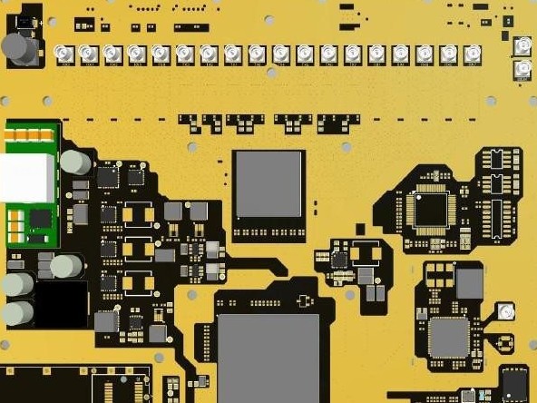
No photograph of the built board published yet; images are CAD renders.
How the platform is offered
Early-access development kit
The board, the Windows PCIe driver (based on the XDMA reference driver) and the host-software prototype with its simulator, as an early-access development kit for university, institute and corporate R&D teams working in their own development facilities. The 8T8R board is intended to combine several narrow-band radios into one coherent eight-channel unit for MIMO and channel-sounding work.
Custom development
Architecture, FPGA firmware, host software and reference designs built to your requirement on this platform — channel counts, bandwidth allocation, on-board processing, interfaces. Scoped and quoted as a project.
8T8R core board — technical specifications
From the v7 product brochure. Product information subject to configuration and customisation.
How the board samples the RF
Eight 14-bit receive ADC channels and eight 14-bit transmit DAC channels sample and generate the RF directly. There is no analogue mixer or local oscillator, so there is no LO leakage or analogue I/Q imbalance to correct; the remaining spurs and noise contributions (converter interleaving, harmonics folding into the band, DAC images, NCO, clock jitter) are still to be characterised. Tuning is done by the digital down-converters and NCOs in the converters, with further processing in the XCKU5P FPGA. The bandwidth delivered per channel is set by the decimation and the JESD204C lane budget, and will be published when it is characterised. 8T8R + 2FB means 8 transmit, 8 receive and 2 feedback channels. The FPGA designs and host library are developed in-house (the Windows driver builds on the XDMA reference driver), which is why the platform is the planned base for our next-generation radar, coverage and monitoring products.
| Parameter | Specification |
|---|---|
| Channel configuration | 8T8R + 2FB: 8 transmit, 8 receive and 2 feedback channels |
| RF architecture | RF direct-sampling transceiver |
| ADC | 8 receive channels, 14-bit · up to 5.8 GSPS (converter maximum) |
| DAC | 8 transmit channels, 14-bit · up to 9.85 GSPS (converter maximum) |
| Signal coverage | Receive 20 MHz – 10 GHz via Nyquist zones (design target); transmit range to be characterised |
| Tuning and bandwidth per channel | Digital down-conversion and NCO in the converters, further processing in the FPGA; bandwidth per channel set by decimation and the JESD204C lane budget, published when characterised |
| FPGA | Kintex UltraScale+ KU5P (XCKU5P) — 475K logic cells, 1,824 DSP slices |
| Converter interface | JESD204C |
| Host interface | PCIe Gen3 ×4 (4 × 8 GT/s, ≈31.5 Gb/s after 128b/130b encoding, before protocol overhead) |
| Optical interface | 2 × SFP+ (16G) |
| Additional interfaces | USB (control), RS232, RS485, extended I/O |
| Operating temperature | −40 °C to +70 °C (design target) |
| Power consumption (typical) | ≤ 40 W (design target) |
| Module size · weight | 165 × 150 × 30 mm · 700 g |
Block diagram and the shared clock domain
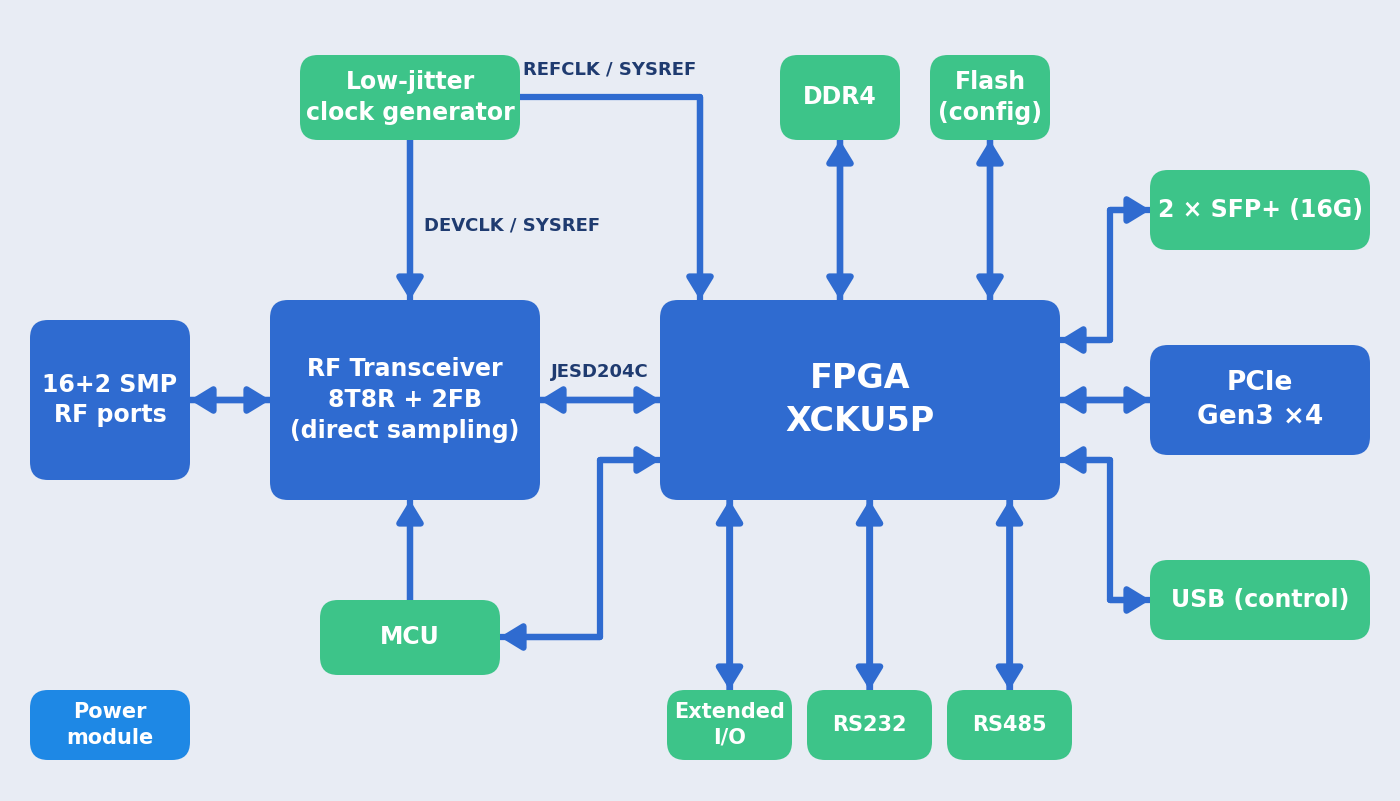
8T8R + 2FB direct-sampling architecture with JESD204C and XCKU5P processing
What eight channels in one clock domain give you
- All eight transmit and eight receive channels share one clock domain
- Measured channel-to-channel figures will be published in the datasheet once characterised
- Per-channel NCO tuning, timed operation on a shared timebase and NCO phase alignment, in the FPGA logic
- Wideband acquisition with processing in the on-board FPGA
Frequency plan
Frequency plan
The 5.8 GSPS ADCs give a first receive Nyquist zone up to 2.9 GHz. Higher bands up to 10 GHz are reached in higher Nyquist zones with band-select filtering chosen per application. Receive zone edges fall at 2.9, 5.8 and 8.7 GHz. The 9.85 GSPS DACs have their first zone edge at 4.925 GHz, and their output response falls towards a null near 9.85 GHz, so the transmit range is still to be characterised. Usable bands are agreed per project.
The bandwidth delivered per channel is set by the decimation in the converters and the JESD204C lane budget; it will be published when characterised. A single receive capture is in any case bounded by one Nyquist zone of 2.9 GHz.
Host interfaces will carry a decimated stream. Rates delivered to the FPGA and to the host are published with the datasheet as they are characterised.
Three generations
The 8T8R core board is the current flagship. The v2 4T4R board hardware is available; the v1 4T4R board is legacy and supplied on request.
Compare the three generations
Scroll the table sideways →
| Gen | FPGA | Channels | Bandwidth per channel | Host | Intended use | Status |
|---|---|---|---|---|---|---|
| v1 | Artix UltraScale+ AU15P | 4T4R | on request | USB 3 | Compact monitoring, radio development | Legacy · on request |
| v2 | Kintex UltraScale+ KU5P (XCKU5P) | 4T4R | on request | USB 3 · PCIe | Spectrum monitoring, wideband recording, custom radios | Hardware available |
| v3 | Kintex UltraScale+ KU5P (XCKU5P) | 8T8R + 2FB | published when characterised | PCIe Gen3 ×4 · 2 × SFP+ (16G) · USB (control) | 6G research, MIMO and beamforming, radar, multi-band monitoring | Flagship · hardware built |
Pictures of the boards
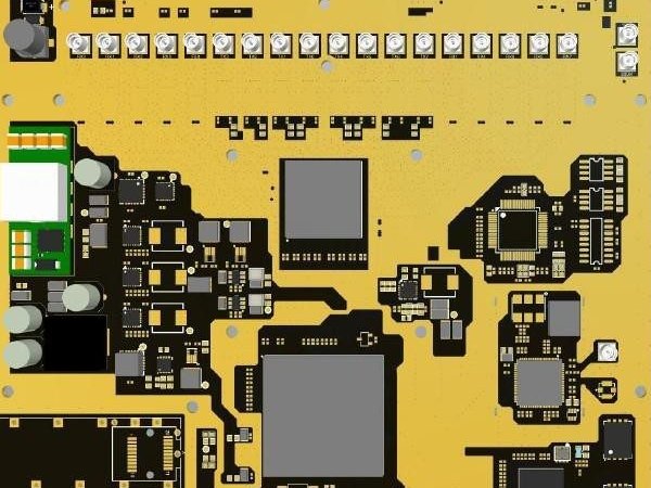
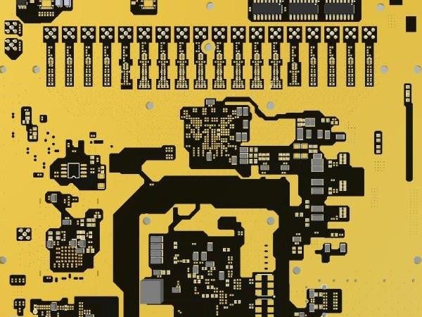
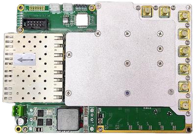
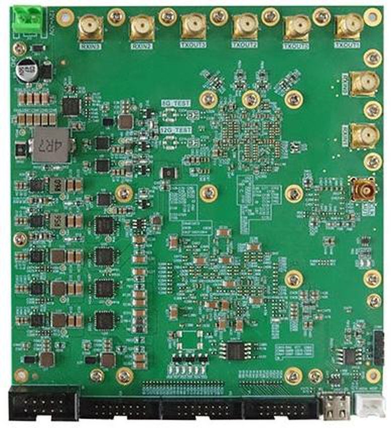
The two 8T8R images are CAD renders of the board.
Software and firmware: what exists today
Start developing before the board arrives
The host-software prototype includes a software simulator of the board. It sits behind the same hardware abstraction layer as the board itself, so application code can be written and tested on a laptop first. The same simulator is the acceptance reference for the FPGA logic.
The FPGA designs and the host stack are developed in-house, so custom work is an engineering task, not a vendor request. The board below lists what is available, what is being written and what is planned.

Our browser-based spectrum monitoring software: sweep, detection and band classification. A recorded sweep of 68 frames, each reduced to 1024 display points across the span, replayed frame by frame; not recorded on the 8T8R board.
Available now · In development · Planned
Available now
- 8T8R board hardware, built: Kintex UltraScale+ KU5P (XCKU5P), direct-sampling ADC and DAC, 8 transmit, 8 receive and 2 feedback channels
- Windows PCIe driver, based on the XDMA reference driver; the streaming data path is in development
- Host-software architecture prototype: a hardware abstraction layer with three back-ends (board protocol, simulator, generic)
- Software simulator of the board, the acceptance reference for the FPGA
- Command-line tool, desktop GUI and automated test suite, part of the prototype
In development
- FPGA logic for the 8T8R board, in four stages
Order of work
- Control plane and timebase
- Single-channel receive path: digital down-conversion, NCO, packetiser
- Eight channels plus transmit, with timed operation and NCO phase alignment
- Enhancements
- PCIe streaming data path
- Production host software
Planned
Host-software items: drivers, framework plug-ins and tools. None of the planned items is released.
Planned items
- Native data plane
- SoapySDR plug-in and GNU Radio module, with an open-source host driver
- Calibration suite
- Record and replay tools
- Linux driver
What the platform is suited to
Wide band, eight channels in one clock domain, programmable fabric, and the fields they are aimed at.
Communications & MIMO · Spectrum monitoring · Radar & imaging
Communications & MIMO research
Channel sounding, 8×8 MIMO, beamforming and phased-array prototyping, custom waveforms for 5G and 6G work. The board is intended to combine several narrow-band radios into one coherent eight-channel unit.
EIGHT CHANNELS · ONE CLOCK DOMAINSpectrum monitoring & direction finding
Wideband occupancy, interference hunting and long-term recording; with eight channels, angle-of-arrival estimation of the source. Power and occupancy only, no content decoding. 5.8 GHz is a receive zone edge; the band plan around it is set per project.
WIDE BAND · EIGHT-CHANNEL ARRAYRadar & imaging
Stepped-frequency and MIMO radar research: ground penetrating radar arrays, through-wall and concrete imaging, non-destructive testing. Our own next-generation array GPR is being developed on this platform.
RAYS GPR ROADMAP →Microwave imaging research
Multistatic stepped-frequency imaging with eight coherent channels and antenna switching, studied in full-wave simulation on head and breast phantoms. Simulation data only.
SIMULATION STUDY · DEMONSTRATION →More application fields
Satellite & GNSS
S-band telemetry and command, X-band downlink reception, multi-constellation GNSS receivers and multi-antenna interference mitigation research. Bands above 2.9 GHz use higher Nyquist zones with filtering agreed per project.
HIGHER NYQUIST ZONES · FILTERING PER PROJECTTest & measurement
Spectrum analysis, multi-channel signal generation and capture, pre-test measurements in the lab: a programmable complement to bench instruments.
EIGHT CHANNELS · PROGRAMMABLEQuantum control research
Synthesis and acquisition in selected sub-bands between 4 and 8 GHz, away from the converter zone edges, for qubit control and readout experiments. Candidate application; suitability to be characterised.
CANDIDATE APPLICATIONNext-generation products planned on the platform
Same FPGA and host code base, three application layers. Stated as a roadmap: none of these is a shipping product yet.
Array ground penetrating radar
Stepped-frequency MIMO array for utility mapping and 3D surveys, processed in RsGprProc. Design stage; to be used first on our own surveys.
Digital channel-selective repeater
In development, no pilot units yet: TETRA and LTE in one unit, remotely configurable band plans, management hosted in the EU or on the customer’s own server, and an open monitoring interface.
Monitoring and direction-finding station
Planned: the browser-based spectrum software on our own boards, with eight-channel angle-of-arrival, for spectrum users who need to find an interferer.
Request documentation or the early-access development kit
The early-access development kit is issued per request to research and development teams. Custom development is scoped from the same conversation. An engineer replies within one working day.
Development kit: what you receive
Development kit: what you receive
- The board
- Power and interface documentation
- Windows PCIe driver, based on the XDMA reference driver
- Host-software prototype with simulator and test suite
- Direct contact with the engineer who writes the firmware
FPGA firmware is delivered in stages as it is completed; early-access users get development builds.
The development kit is supplied for use in the recipient's own development facilities. Deployment products are delivered as scoped projects.